
Introduction
For the most of the twentieth century, a photosensitive chemical emulsion spread on film was used to reproduce images from the optical microscope. It has only been in the past decade that improvements in electronic camera and computer technology have made digital imaging faster, cheaper, and far more accurate to use than conventional photography. A wide range of new and exciting techniques have subsequently been developed that enable researchers to probe deeper into tissues, observe extremely rapid biological processes in living cells, and obtain quantitative information about spatial and temporal events on a level approaching the single molecule. The imaging device is one of the most critical components in optical microscopy because it determines at what level fine specimen detail may be detected, the relevant structures resolved, and/or the dynamics of a process visualized and recorded. The range of light detection methods and the wide variety of imaging devices currently available to the microscopist make the equipment selection process difficult and often confusing. This discussion is intended to aid in understanding the basics of light detection, the fundamental properties of digital images, and the criteria relevant to selecting a suitable detector for specific applications.
Recording images with the microscope dates back to the earliest days of microscopy. The first single lens instruments, developed by Dutch scientists Antoni van Leeuwenhoek and Jan Swammerdam in the late 1600s, were used by these pioneering investigators to produce highly detailed drawings of blood, microorganisms, and other minute specimens. British scientist Robert Hooke engineered one of the first compound microscopes and used it to write Micrographia, his hallmark volume on microscopy and imaging published in 1665. The microscopes developed during this period were incapable of projecting images, and observation was limited to close visualization of specimens through the eyepiece. True photographic images were first obtained with the microscope in 1835 when William Henry Fox Talbot applied a chemical emulsion process to capture photomicrographs at low magnification. Between 1830 and 1840 there was an explosive growth in the application of photographic emulsions to recording microscopic images. For the next 150 years, the art and science of capturing images through the microscope with photographic emulsions co-evolved with advancements in film technology. During the late 1800s and early 1900s, Carl Zeiss and Ernst Abbe perfected the manufacture of specialized optical glass and applied the new technology to many optical instruments, including compound microscopes.
The dynamic imaging of biological activity was introduced in 1909 by French doctorial student Jean Comandon, who presented one of the earliest time lapse videos of syphilis producing spirochaetes. Comandon's technique enabled movie production of the microscopic world. Between 1970 and 1980 researchers coupled tube based video cameras with microscopes to produce time lapse image sequences and real-time videos. In the 1990s the tube camera gave way to solid state technology and the area array charge coupled device (CCD), heralding a new era in photomicrography. Current terminology referring to the capture of electronic images with the microscope is digital or electronic imaging.
back to top ^Digital Image Acquisition: Analog to Digital Conversion
Regardless of whether light focused on a specimen ultimately impacts on the human retina, a film emulsion, a phosphorescent screen or the photodiode array of a CCD, an analog image is produced. These images can contain a wide spectrum of intensities and colors. Images of this type are referred to as continuous tone because the various tonal shades and hues blend together without disruption, to generate a diffraction limited reproduction of the original specimen. Continuous tone images accurately record image data by using a sequence of electrical signal fluctuations that vary continuously throughout the image.
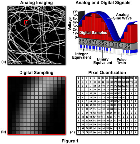
As we view them, images are generally square or rectangular in dimension thus each pixel is represented by a coordinate pair with specific x and y values, arranged in a typical Cartesian coordinate system (Figure 1c). The x coordinate specifies the horizontal position or column location of the pixel, while the y coordinate indicates the row number or vertical position. Thus, a digital image is composed of a rectangular or square pixel array representing a series of intensity values that is ordered by an (x, y) coordinate system. In reality, the image exists only as a large serial array of data values that can be interpreted by a computer to produce a digital representation of the original scene.
The horizontal to vertical dimension ratio of a digital image is known as the aspect ratio and can be calculated by dividing the image width by the height. The aspect ratio defines the geometry of the image. By adhering to a standard aspect ratio for display of digital images, gross distortion of the image is avoided when the images are displayed on remote platforms. When a continuous tone image is sampled and quantized, the pixel dimensions of the resulting digital image acquire the aspect ratio of the original analog image. It is important that each pixel has a 1:1 aspect ratio (square pixels) to ensure compatibility with common digital image processing algorithms and to minimize distortion.
back to top ^Spatial Resolution in Digital Images
The quality of a digital image, or image resolution, is determined by the total number of pixels and the range of brightness values available for each pixel. Image resolution is a measure of the degree to which the digital image represents the fine details of the analog image recorded by the microscope. The term spatial resolution is reserved to describe the number of pixels utilized in constructing and rendering a digital image. This quantity is dependent upon how finely the image is sampled during digitization, with higher spatial resolution images having a greater number of pixels within the same physical image dimensions. Thus, as the number of pixels acquired during sampling and quantization of a digital image increases, the spatial resolution of the image also increases.
The optimum sampling frequency, or number of pixels utilized to construct a digital image, is determined by matching the resolution of the imaging device and the computer system used to visualize the image. A sufficient number of pixels should be generated by sampling and quantization to dependably represent the original image. When analog images are inadequately sampled, a significant amount of detail can be lost or obscured, as illustrated by the diagrams in Figure 2. The analog signal presented in Figure 2(a) shows the continuous intensity distribution displayed by the original image, before sampling and digitization, when plotted as a function of sample position. When 32 digital samples are acquired (Figure 2(b)), the resulting image retains a majority of the characteristic intensities and spatial frequencies present in the original analog image.
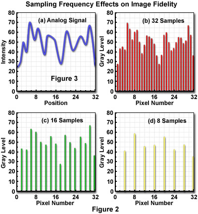
When the sampling frequency is reduced as in Figure 2(c) and (d), frequencies present in the original image are missed during analog-to-digital (A/D) conversion and a phenomenon known as aliasing develops. Figure 2(d) illustrates the digital image with the lowest number of samples, where aliasing has produced a loss of high spatial frequency data while simultaneously introducing spurious lower frequency data that don't actually exist.
The spatial resolution of a digital image is related to the spatial density of the analog image and the optical resolution of the microscope or other imaging device. The number of pixels and the distance between pixels (the sampling interval) in a digital image are functions of the accuracy of the digitizing device. The optical resolution is a measure of the ability of the optical lens system (microscope and camera) to resolve the details present in the original scene. Optical resolution is affected by the quality of the optics, image sensor, and supporting electronics. Spatial density and the optical resolution determine the spatial resolution of the image. Spatial resolution of the image is limited solely by spatial density when the optical resolution of the imaging system is superior to the spatial density.
All of the details contained in a digital image are composed of brightness transitions that cycle between various levels of light and dark. The cycle rate between brightness transitions is known as the spatial frequency of the image, with higher rates corresponding to higher spatial frequencies. Varying levels of brightness in minute specimens observed through the microscope are common, with the background usually consisting of a uniform intensity and the specimen exhibiting a larger range of brightness levels.
The numerical value of each pixel in the digital image represents the intensity of the optical image averaged over the sampling interval. Thus, background intensity will consist of a relatively uniform mixture of pixels, while the specimen will often contain pixels with values ranging from very dark to very light. Features seen in the microscope that are smaller than the digital sampling interval will not be represented accurately in the digital image. The Nyquist criterion requires a sampling interval equal to twice the highest spatial frequency of the specimen to accurately preserve the spatial resolution in the resulting digital image. If sampling occurs at an interval beneath that required by the Nyquist criterion, details with high spatial frequency will not be accurately represented in the final digital image. The Abbe limit of resolution for optical images is approximately 0.22 micrometers (using visible light), meaning that a digitizer must be capable of sampling at intervals that correspond in the specimen space to 0.11 micrometers or less. A digitizer that samples the specimen at 512 pixels per horizontal scan line would have to produce a maximum horizontal field of view of 56 micrometers (512 x 0.11 micrometers) in order to conform to the Nyquist criterion. An interval of 2.5 to 3 samples for the smallest resolvable feature is suggested to ensure adequate sampling for high resolution imaging.
A serious sampling artifact known as spatial aliasing (undersampling) occurs when details present in the analog image or actual specimen are sampled at a rate less than twice their spatial frequency. When the pixels in the digitizer are spaced too far apart compared to the high frequency detail present in the image, the highest frequency information masquerades as low spatial frequency features that are not actually present in the digital image. Aliasing usually occurs as an abrupt transition when the sampling frequency drops below a critical level, which is about 25 percent below the Nyquist resolution limit. Specimens containing regularly spaced, repetitive patterns often exhibit moiré fringes that result from aliasing artifacts induced by sampling at less than 1.5 times the repetitive pattern frequency.
back to top ^The Contrast Transfer Function
Contrast can be understood as a measure of changes in image signal intensity (ΔI) in relation to the average image intensity (I) as expressed by the following equation:
C = ΔI/I(1)
Of primary consideration is the fact that an imaged object must differ in recorded intensity from that of its background in order to be perceived. Contrast and spatial resolution are closely related and both are requisite to producing a representative image of detail in a specimen. The contrast transfer function (CTF) is analogous to the modulation transfer function (MTF), a measure of the microscope's ability to reproduce specimen contrast in the intermediate image plane at a specific resolution. The MTF is a function used in electrical engineering to relate the amount of modulation present in an output signal to the signal frequency. In optical digital imaging systems, contrast and spatial frequency are correlates of output modulation and signal frequency in the MTF. The CTF characterizes the information transmission capability of an optical system by graphing percent contrast as a function of spatial frequency as shown in Figure 3, which illustrates the CTF and distribution of light waves at the objective rear focal plane. The objective rear aperture presented in Figure 3(a) demonstrates the diffraction of varying wavelengths that increase in periodicity moving from the center of the aperture towards the periphery, while the CTF in Figure 3(b) indicates the Rayleigh limit of optical resolution.
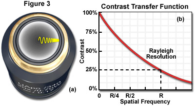
Spatial frequency can be defined as the number of times a periodic feature recurs in a given unit space or interval. The intensity recorded at zero spatial frequency in the CTF is a quantification of the average brightness of the image. Since contrast is diffraction limited, spatial frequencies near zero will have high contrast (approximately 100 percent) and those with frequencies near the diffraction limit will have lower recorded contrast in the image. As the CTF graph in Figure 3 illustrates, the Rayleigh Criterion is not a fixed limit but rather, the spatial frequency at which the contrast has dropped to about 25 percent. The CTF can therefore provide information about how well an imaging system can represent small features in a specimen.
The CTF can be determined for any functional component of the imaging system and is a performance measure of the imaging system as a whole. System performance is evaluated as the product of the CTF curves determined for each component. Therefore, it will be lower than that of any of the individual components. Small features that have limited contrast to begin with will become even less visible as the image passes through successive components of the system. The lowest CTFs are typically observed in the objective and CCD. The analog signal produced by the CCD can be modified before being passed to the digitizer to increase contrast using the analog gain and offset controls. Once the image has been digitally encoded, changes in magnification and concomitant adjustments of pixel geometry can result in improvement of the overall CTF.
back to top ^Image Brightness and Bit Depth
The brightness of a digital image is a measure of relative intensity values across the pixel array, after the image has been acquired with a digital camera or digitized by an A/D converter. Brightness should not be confused with radiant intensity, which refers to the magnitude or quantity of light energy actually reflected from or transmitted through the object being imaged. As concerns digital image processing, brightness is best described as the measured intensity of all the pixels comprising the digital image after it has been captured, digitized, and displayed. Pixel brightness is important to digital image processing because, other than color, it is the only variable that can be utilized by processing techniques to quantitatively adjust the image.
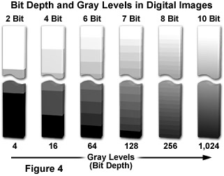
Regardless of capture method, an image must be digitized to convert the specimen's continuous tone intensity into a digital brightness value. The accuracy of the digital value is directly proportional to the bit depth of the digitizing device. If two bits are utilized, the image can only be represented by four brightness values or levels (2 x 2). Likewise, if three or four bits are processed, the corresponding images have eight (2 x 2 x 2) and 16 (2 x 2 x 2 x 2) brightness levels, as shown in Figure 4, which illustrates the correlation between bit depth and the number of gray levels in digital images. If two bits are utilized, the image can only be represented by four brightness values or levels. Likewise, if three or four bits are processed, the corresponding images have eight and 16 brightness levels, respectively. In all of these cases, level 0 represents black, while the top level represents white, and each intermediate level is a different shade of gray.
The grayscale or brightness range of a digital image consists of gradations of black, white, and gray brightness levels. The greater the bit depth the more grey levels are available to represent intensity changes in the image. For example, a 12-bit digitizer is capable of displaying 4,096 gray levels (2 x 10¹²) when coupled to a sensor having a dynamic range of 72 decibels (dB). When applied in this sense, dynamic range refers to the maximum signal level with respect to noise that the CCD sensor can transfer for image display. It can be defined in terms of pixel signal capacity and sensor noise characteristics. Similar terminology is used to describe the range of gray levels utilized in creating and displaying a digital image. This usage is relevant to the intrascene dynamic range.
The term bit depth refers to the binary range of possible grayscale values used by the analog to digital converter, to translate analog image information into discrete digital values capable of being read and analyzed by a computer. For example, the most popular 8-bit digitizing converters have a binary range of 256 (2 x 10⁸) possible values and a 16-bit converter has 65,536 (2 x 10¹⁶) possible values. The bit depth of the A/D converter determines the size of the gray scale increments, with higher bit depths corresponding to a greater range of useful image information available from the camera.
The number of grayscale levels that must be generated in order to achieve acceptable visual quality should be enough that the steps between individual gray values are not discernible to the human eye. The just noticeable difference in intensity of a gray level image for the average human eye is about two percent under ideal viewing conditions. At most, the human eye can distinguish about 50 discrete shades of gray within the intensity range of a video monitor, suggesting that the minimum bit depth of an image should be between 6 and 7 bits.
Digital images should have at least 8-bit to 10-bit resolution to avoid producing visually obvious gray level steps in the enhanced image when contrast is increased during image processing. The number of pixels and gray levels necessary to adequately describe an image is dictated by the physical properties of the specimen. Low contrast, high resolution images often require a significant number of gray levels and pixels to produce satisfactory results, while other high contrast and low resolution images (such as a line grating) can be adequately represented with a significantly lower pixel density and gray level range. Finally, there is a trade off in computer performance between contrast, resolution, bit depth, and the speed of image processing algorithms.
back to top ^Image Histograms
Grey-level or image histograms provide a variety of useful information about the intensity or brightness of a digital image. In a typical histogram, the pixels are quantified for each grey level of an 8-bit image. The horizontal axis is scaled from 0 to 255 and the number of pixels representing each grey level is graphed on the vertical axis. Statistical manipulation of the histogram data allows the comparison of images in terms of their contrast and intensity. The relative number of pixels at each grey level can be used to indicate the extent to which the grey level range is being utilized by a digital image. Pixel intensities are well distributed among grey levels in an image having normal contrast and indicate a large intrascene dynamic range. In low contrast images only a small portion of available grey levels are represented and intrascene dynamic range is limited. When pixel intensities are distributed among high and low grey levels, leaving the intermediate levels unpopulated, there is an excess of black and white pixels and contrast is typically high.
back to top ^Properties of Charge Coupled Device Cameras
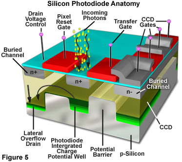
The fundamental processes involved in creating an image with a CCD camera include: exposure of the photodiode array elements to incident light, conversion of accumulated photons to electrons, organization of the resulting electronic charge in potential wells and, finally, transfer of charge packets through the shift registers to the output amplifier. Charge output from the shift registers is converted to voltage and amplified prior to digitization in the A/D converter. Different structural arrangement of the photodiodes and photocapacitors result in a variety of CCD architectures. Some of the more commonly used configurations include frame transfer (FT), full frame (FF), and interline (IL) types. Modifications to the basic architecture such as electron multiplication, back thinning/illumination and the use of microlenticular (lens) arrays have helped to increase the sensitivity and quantum efficiency of CCD cameras. The basic structure of a single metal oxide semiconductor (MOS) element in a CCD array is illustrated in Figure 5. The substrate is a p/n type silicon wafer insulated with a thin layer of silicon dioxide (approximately 100 nanometers) that is applied to the surface of the wafer. A grid pattern of electrically conductive, optically transparent, polysilicon squares or gate electrodes are used to control the collection and transfer of photoelectrons through the array elements.
After being accumulated in a CCD during the exposure interval, photoelectrons accumulate when a positive voltage (0-10 volts) is applied to an electrode. The applied voltage leads to a hole-depleted region beneath the electrode known as a potential well. The number of electrons that can accumulate in the potential well before their charge exceeds the applied electric field is known as the full well capacity. The full well capacity depends on pixel size. A typical full well capacity for CCDs used in fluorescence microscopy is between 20,000 and 40,000 photons. Excessive exposure to light can lead to saturation of the pixels where photons spill over into adjacent pixels and cause the image to smear or bloom. In many modern CCDs, special "anti-blooming" channels are incorporated to prevent the excess electrons from affecting the surrounding pixels. The benefit of anti-blooming generally outweighs the decrease in full well capacity that is a side effect of the feature.
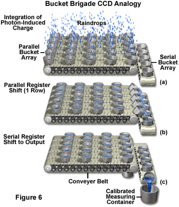
The length of time electrons are allowed to accumulate in a potential well is a specified integration time controlled by a computer program. When a voltage is applied at a gate, electrons are attracted to the electrode and move to the oxide/silicon interface where they collect in a 10nm thick region until the voltages at the electrodes are cycled or clocked. Different bias voltages applied to the gate electrodes control whether a potential well or barrier will form beneath a particular gate. During charge transfer the charge packet held in the potential well is transferred from pixel to pixel in a cycling or clocking process often explained by analogy to a bucket brigade as shown in Figure 6. In the bucket brigade analogy, raindrops are first collected in a parallel bucket array (Figure 6(a)), and then transferred in parallel to the serial output register (Figure 6(b)). The water accumulated in the serial register is output, one bucket at a time, to the output node (calibrated measuring container). Depending on CCD type, various clocking circuit configurations may be used. Three phase clocking schemes are commonly used in scientific cameras.
The grid of electrodes forms a two dimensional, parallel register. When a programmed sequence of changing voltages is applied to the gate electrodes the electrons can be shifted across the parallel array. Each row in the parallel register is sequentially shifted into the serial register. The contents of the serial register are shifted one pixel at a time into the output amplifier where a signal proportional to each charge packet is produced. When the serial register is emptied the next row in the parallel register is shifted and the process continues until the parallel register has been emptied. This function of the CCD is known as charge transfer or readout and relies on the efficient transfer of charge from the photodiodes to the output amplifier. The rate at which image data are transferred depends on both the bandwidth of the output amplifier and the speed of the A/D converter.
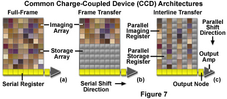
Charge coupled device cameras use a variety of architectures to accomplish the tasks of collecting photons and moving the charge out of the registers and into the readout amplifier. The simplest CCD architecture is known as Full Frame (FF) (see Figure 7a). This configuration consists of a parallel photodiode shift register and a serial shift register. Full frame CCDs use the entire pixel array to simultaneously detect incoming photons during exposure periods and thus have a 100-percent fill factor. Each row in the parallel register is shifted into the serial register. Pixels in the serial register are read out in discrete packets until all the information in the array has been transferred into the readout amplifier. The output amplifier then produces a signal proportional to that of each pixel in the array. Since the parallel array is used both to detect photons and transfer the electronic data, a mechanical shutter or synchronized strobe light must be used to prevent constant illumination of the photodiodes. Full frame CCDs typically produce high resolution, high density images but can be subject to significant readout noise.
Frame Transfer (FT) architecture (Figure 7b) divides the array into a photoactive area and a light shielded or masked array, where the electronic data are stored and transferred to the serial register. Transfer from the active area to the storage array depends upon the array size but can take less than half a millisecond. Data captured in the active image area are shifted quickly to the storage register where they are read out row by row into the serial register. This arrangement allows simultaneous readout of the initial frame and integration of the next frame. The main advantage of frame transfer architecture is that it eliminates the need to shutter during the charge transfer process and thus increases the frame rate of the CCD.
For every active row of pixels in an Interline (IL) array (Figure 7c) there is a corresponding masked transfer row. The exposed area collects image data and following integration, each active pixel rapidly shifts its collected charge to the masked part of the pixel. This allows the camera to acquire the next frame while the data are shifted to charge transfer channels. Dividing the array into alternating rows of active and masked pixels permits simultaneous integration of charge potential and readout of the image data. This arrangement eliminates the need for external shuttering and increases the device speed and frame rate. The incorporation of a microscopic lens partially compensates for the reduced light gathering ability caused by pixel masking. Each lens directs a portion of the light that would otherwise be reflected by the aluminum mask to the active area of the pixel.
Readout speed can be enhanced by defining one or more sub-arrays that represent areas of interest in the specimen. The reduction in pixel count results in faster readout of the data. The benefit of this increased readout rate occurs without a corresponding increase in noise, unlike the situation of simply increasing clock speed. In a clocking routine known as binning, charge is collected from a specified group of adjacent pixels and the combined signal is shifted into the serial register. The size of the binning array is usually selectable and can range from 2 x 2 pixels to most of the CCD array. The primary reasons for using binning are to improve the signal noise ratio and dynamic range. These benefits come at the expense of spatial resolution. Therefore, binning is commonly used in applications where resolution of the image is less important than rapid throughput and signal improvement.
In addition to micro lens technology a number of physical modifications have been made to CCDs to improve camera performance. Instruments used in contemporary biological research must be able to detect weak signals typical of low fluorophore concentrations and tiny specimen volumes, cope with low excitation photon flux and achieve the high speed and sensitivity required for imaging rapid cellular kinetics. The demands imposed on detectors can be considerable: ultra-low detection limits, rapid data acquisition and generation of a signal that's distinguishable from the noise produced by the device.
Most contemporary CCD enhancement is a result of backthinning and/or gain register electron multiplication. Backthinning avoids the loss of photons that are either absorbed or reflected from the overlying films on the pixels in standard CCDs. Also, electrons created at the surface of the silicon by ultraviolet and blue wavelengths are often lost due to recombination at the oxide silicon interface, thus rendering traditional CCD chips less sensitive to high frequency incident light. Using an acid etching technique, the CCD silicon wafer can be uniformly thinned to about 10-15 micrometers. Incident light is directed onto the back side of the parallel register away from the gate structure. A potential accumulates on the surface and directs the generated charge to the potential wells. Back thinned CCDs exhibit photon sensitivity throughout a wide range of the electromagnetic spectrum, typically from ultraviolet to near infrared wavelengths. Back thinning can be used with FF or FT architectures, in combination with solid state electron multiplication devices, to increase quantum efficiency to above 90 percent.
The electron multiplying CCD (EMCCD) is a modification of the conventional CCD in which an electron multiplying register is inserted between the serial register output and the charge amplifier. This multiplication register or gain register is designed with an extra grounded phase that creates a high field region and a higher voltage (35-45 volts) than the standard CCD horizontal register (5-15 volts). Electrons passing through the high field region are multiplied as a result of an approximately 1-percent probability that an electron will be produced as a result of collision. The multiplication register consists of 4 gates that use clocking circuits to apply potential differences (35-40 volts) and generate secondary electrons by the process of impact ionization. Impact ionization occurs when an energetic charge carrier loses energy during the creation of other charge carriers. When this occurs in the presence of an applied electric field an avalanche breakdown process produces a cascade of secondary electrons (gain) in the register. Despite the small (approximately 1 percent) probability of generating a secondary electron the large number of pixels in the gain register can result in the production of electrons numbering in the hundreds or thousands.
Traditional slow scan CCDs achieve high sensitivity and high speed but do so at the expense of readout rate. Readout speed is constrained in these cameras by the charge amplifier. In order to attain high speed, the bandwidth of the charge amplifier must be as wide as possible. However, as the bandwidth increases so too does the amplifier noise. The typically low bandwidths of slow scan cameras means they can only be read out at lower speeds (approximately 1 MHz). EMCCDs side step this constraint by amplifying the signal prior to the charge amplifier, effectively reducing the relative readout noise to less than one electron, thus providing both low detection limit and high speed. EMCCDs are therefore able to produce low light images rapidly, with good resolution, a large intensity range and a wide dynamic range.
back to top ^CCD Performance Measures: Camera Sensitivity
The term sensitivity, with respect to CCD performance, can be interpreted differently depending on the incident light level used in a particular application. In imaging scenarios where signal levels are low, such as in fluorescence microscopy, sensitivity refers to the ability of the CCD to detect weak signals. In high light level applications (such as brightfield imaging of stained specimens), performance may be measured as the ability to determine small changes in the bright images. In the case of low light levels, the camera noise is the limiting factor to sensitivity but, in the case of high light levels, the signal noise becomes the limiting factor.
The signal-to-noise ratio (SNR) of a camera can measure the ratio of signal levels that a camera can detect in a single exposure but it cannot determine the sensitivity to weak light or the sensitivity to change in large signals unless the values in the ratio are known. A camera with 2 electrons of camera noise and a 20,000-electron full well capacity will have the same SNR (10,000:1) as a camera with 20 electrons camera of noise and a 200,000-electron full well capacity. However, the first camera will be much more sensitive to low signals and the second camera will offer much better sensitivity to small changes in a large signal. The difference is in the type of noise for each application. The low-light camera is limited by the camera noise, 2 electrons in this case, which means a minimum of about 5 signal electrons would be detectable. High light level sensitivity is limited by the noise of the signal, which in this case is the square root of 200,000 (447 electrons), representing a detectable change of about 0.2 percent of the signal.
Sensitivity depends on the limiting noise factor and in every situation there is a rough measure of CCD device performance is the ratio of incident light signal to that of the combined noise of the camera. Signal (S) is determined as a product of input light level (I), quantum efficiency (QE) and the integration time (T) measured in seconds.
S = I × QE × T(2)
There are numerous types and sources of noise generated throughout the digital imaging process. Its amount and significance often depend on the application and type of CCD used to create the image. The primary sources of noise considered in determining the ratio are statistical (shot noise), thermal noise (dark current) and preamplification or readout noise, though other types of noise may be significant in some applications and types of camera. Total noise is usually calculated as the sum of readout noise, dark current and statistical noise in quadrature as follows:
Total Noise =  Read Noise2 + Dark Noise2 + Shot Noise2(3)
Preamplification or read noise is produced by the readout electronics of the CCD. Read noise is comprised of two primary types or sources of noise, related to the operation of the solid state electrical components of the CCD. White noise originates in the metal oxide semiconductor field effect transistor (MOSFET) of the output amplifier, where the MOSFET resistance generates thermal noise. Flicker noise, also known as 1/f noise, is also a product of the output amplifier that originates in the material interface between the silicon and silicon dioxide layers of the array elements.
Thermal noise or dark current is generated similarly, as a result of impurities in the silicon that allow energetic states within the silicon band gap. Thermal noise is generated within surface states, in the bulk silicon and in the depletion region, though most are produced at surface states. Dark current is inherent to the operation of semiconductors as thermal energy allows electrons to undergo a stepped transition from the valence band to the conduction band where they are added to the signal electrons and measured by the detector. Thermal noise is most often reduced by cooling the CCD. This can be accomplished using liquid nitrogen or a thermoelectric (Peltier) cooler. The former method places the CCD in a nitrogen environment where the temperature is so low that significant thermal noise is eliminated. Thermoelectric cooling is commonly used to reduce the contribution of thermal noise to total camera noise. A Peltier type cooler uses a semiconductor sandwiched between two metal plates. When a current is applied the device acts like a heat pump and transfers heat from the CCD.
Amplification noise occurs in the gain registers of EMCCDs and is often represented by a quantity known as the Noise Factor. For low light imaging systems the noise introduced by the multiplicative process or gain can be an important performance parameter. The electron multiplication process amplifies weak signals above the noise floor enabling detection of signals as low as those produced by single photon events, in some cases. In any process in which a signal is amplified, noise added to the signal is also amplified. For this reason it is important to cool EMCCDs to reduce dark current and its associated shot noise.
Any time we undertake to quantify photons or photoelectric events there is inherent uncertainty in the measurement that is due to the quantum nature of light. The absorption of photons is a quantum mechanical event and thus the number of photons absorbed varies according to a Poisson distribution. The accuracy of determinations of the number of photons absorbed by a particular pixel is fundamentally restrained by this inherent statistical error. This uncertainty is referred to as Poisson, statistical or shot noise, and is given by the square root of the signal or number of photoelectrons detected. In a low light fluorescence application, the mean value of the brightest pixels might be as low as 16 photons. Due to statistical uncertainty or Poisson noise, the actual number of photoelectrons collected in a potential well during an integration period could vary between 12 and 20 (16 ± 4). In mean values representing lower specimen signal levels, the uncertainty becomes more significant. For example, if the mean value is only 4 photoelectrons, the percentage of the signal representing statistical noise jumps to 50 percent (4 ± 2). Poisson or shot noise is an inherent physical limitation. Statistical noise decreases as signal increases and so can only be reduced by increasing the number of events counted. Although quantum efficiency is often considered separately from noise, a value indicating reduced numbers of quantum mechanical events implies an increase in statistical or Poisson noise.
Quantum efficiency (QE) is a measure of camera performance that determines the percentage of photons that are detected by a CCD. It is a property of the photovoltaic response and summarized by the following equation:
QE = ne/np(4)
where the quantum efficiency is equal to the number of electron hole pairs generated as determined by the number of photoelectrons detected (ne) divided by the average number of photons (np) incident on the pixel. Quantum efficiency will always be less than one.
The number of photoelectrons generated is contingent upon the photovoltaic response of the silicon element to the incident photons and depends on a number of conditions. The amount of charge created during a photon silicon interaction depends on a number of factors that include the absorption coefficient and diffusion length. The absorption coefficient of silicon varies as longer wavelengths penetrate further into the silicon substrate than do shorter wavelengths. Above a critical wavelength (greater than 1100 nanometers), photons are not energetic enough to induce the photoelectric effect. Photons in the 450 to 700 nanometer range are absorbed in the location of potential well and in the bulk silicon substrate. The QE of photons absorbed in the depletion area approaches 100 percent while those elsewhere in the substrate may release electrons that move less efficiently.
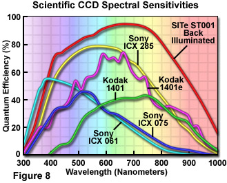
The spectral sensitivity of a CCD depends on the QE of the photoactive elements over the range of near UV to near infrared wavelengths, as illustrated in Figure 8. Modifications made to CCDs to increase performance have led to high QE in the blue green portion of the spectrum. Back thinned CCDs can exhibit quantum efficiencies of greater than 90 percent, eliminating loss due to interaction with the charge transfer channels.
A measure of CCD performance proposed by James Pawley is known as the intensity spread function (ISF) and measures the amount of error due to statistical noise in an intensity measurement. The ISF relates the number measured by the A/D converter to the brightness of a single pixel. The ISF for a particular detector is determined first by making a series of measurements of a single pixel in which the source illumination is uniform and the integration periods identical. The data are then plotted as a histogram and the mean number of photons and the value at the full width half maximum (FWHM) point (the standard deviation) are determined.
The ISF is equal to the mean divided by the FWHM calculated as the standard deviation. The value is expressed as photons meaning it has been corrected for QE and the known proportional relationship between photoelectrons and their representative numbers stored in memory. The quantity that is detected and digitized is proportional to the number of photoelectrons rather than photons. The ISF is thus a measure of the amount of error in the output signal due to statistical noise that increases as the QE (the ratio of photoelectrons to photons) decreases. The statistical error represents the minimum noise level attainable in an imaging system where readout and thermal noise have been adequately reduced.
The conversion of incident photons to an electronic output signal is a fundamental process in the CCD. The ideal relationship between the light input and the final digitized output is linear. As a performance measure, linearity describes how well the final digital image represents the actual features of the specimen. The specimen features are well represented when the detected intensity value of a pixel is linearly related to the stored numerical value and to the brightness of the pixel in the image display. Linearity measures the consistency with which the CCD responds to photonic input over its well depth. Most modern CCDs exhibit a high degree of linear conformity, but deviation can occur as pixels near their full well capacity. As pixels become saturated and begin to bloom or spill over into adjacent pixels or charge transfer channels the signal is no longer affected by the addition of further photons and the system becomes non linear.
Quantitative evaluation of CCD linearity can be performed by generating sets of exposures with increasing exposure times using a uniform light source. The resulting data are plotted with the mean signal value as a function of exposure (integration) time. If the relationship is linear, a 1 second exposure that produces about 1000 electrons predicts that a 10-second exposure will produce about 10,000 electrons. Deviations from linearity are frequently measured in fractions of a percent but no system is perfectly linear throughout its entire dynamic range. Deviation from linearity is particularly important in low light, quantitative applications and for performing flat field corrections. Linearity measurements differ among manufacturers and may be reported as a percentage of conformance to or deviation from the ideal linear condition.
In low-light imaging applications, the fluorescent signal is about a million times weaker than the excitation light. The signal is further limited in intensity by the need to minimize photobleaching and phototoxicity. When quantifying the small number of photons characteristic of biological fluorescent imaging, the process is photon starved but also subject to the statistical uncertainty associated with enumerating quantum mechanical events. The measurement of linearity is further complicated by the fact that the amount of uncertainty increases with the square root of the intensity. This means that the statistical error is largest in the dimmest regions of the image. Manipulating the data using a deconvolution algorithm is often the only way to address this problem in photon limited imaging applications.
back to top ^Multidimensional Imaging
The term multidimensional imaging can be used to describe three-dimensional imaging (3D; volume), four-dimensional imaging (4D; volume and time) or imaging in 5 or more dimensions (5D, 6D, etc., volume, time, wavelength), each representing a combination of different variables. Modern bioscience applications increasingly require optical instruments and digital image processing systems capable of capturing quantitative, multidimensional information about dynamic, spatially complex specimens. Multidimensional, quantitative image analysis has become essential to a wide assortment of bioscience applications. The imaging of sub-resolution objects, rapid kinetics and dynamic biological processes present technical challenges for instrument manufacturers to produce ultra sensitive, extremely fast and accurate image acquisition and processing devices.
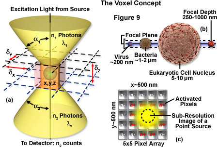
The image produced by the microscope and projected onto the surface of the detector is a two dimensional representation of an object that exists in three dimensional space. As discussed in Part I, the image is divided into a two dimensional array of pixels, represented graphically by an x and y axis. Each pixel is a typically square area determined by the lateral resolution and magnification of the microscope as well as the physical size of the detector array. Similar to the pixel in 2D imaging, a volume element or voxel, having dimensions defined by x, y and z axes, is the basic unit or sampling volume in 3D imaging. A voxel represents an optical section, imaged by the microscope, that is comprised of the area resolved in the x-y plane and a distance along the z axis defined by the depth of field, as illustrated in Figure 9. To illustrate the voxel concept (Figure 9), a sub-resolution fluorescent point object can be described in three dimensions with a coordinate system, as illustrated in Figure 9(a). The typical focal depth of an optical microscope is shown relative to the dimensions of a virus, bacteria, and mammalian cell nucleus in Figure 9(b), whereas Figure 9(c) depicts a schematic drawing of a sub-resolution point image projected onto a 25-pixel array. Activated pixels (those receiving photons) span a much larger dimension than the original point source.
The depth of field is a measurement of object space parallel with the optical axis. It describes the numerical aperture-dependent, axial resolution capability of the microscope objective and is defined as the distance between the nearest and farthest objects in simultaneous focus. Numerical aperture (NA) of a microscope objective is determined by multiplying the sine of one-half of the angular aperture by the refractive index of the imaging medium. Lateral resolution varies inversely with the first power of the NA, whereas axial resolution is inversely related to the square of the NA. The NA therefore affects axial resolution much more so than lateral resolution. While spatial resolution depends only on NA, voxel geometry depends on the spatial resolution as determined by the NA and magnification of the objective, as well as the physical size of the detector array. With the exception of multiphoton imaging, which uses femtoliter voxel volumes, widefield and confocal microscopy are limited to dimensions of about 0.2 micrometers x 0.2 micrometers x 0.4 micrometers based on the highest NA objectives available.
Virus sized objects that are smaller than the optical resolution limits can be detected but are poorly resolved. In thicker specimens, such as cells and tissues, it is possible to repeatedly sample at successively deeper layers so that each optical section contributes to a z series (or z stack). Microscopes that are equipped with computer controlled step motors acquire an image, then adjust the fine focus according to the sampling parameters, take another image, and continue until a large enough number of optical sections have been collected. The step size is adjustable and will depend, as for 2D imaging, on appropriate Nyquist sampling. The axial resolution limit is larger than the limit for lateral resolution. This means that the voxel may not be an equal-sided cube and will have a z dimension that can be several times greater than the x and y dimensions. For example, a specimen can be divided into 5-micrometers thick optical sections and sampled at 20-micrometer intervals. If the x and y dimensions are 0.5 micrometers x 0.5 micrometers then the resulting voxel will be 40 times longer than it is wide.
Three dimensional imaging can be performed with conventional widefield fluorescence microscopes equipped with a mechanism to acquire sequential optical sections. Objects in a focal plane are exposed to an illumination source and light emitted from the fluorophore is collected by the detector. The process is repeated at fine focus intervals along the z axis, often hundreds of times, and a sequence of optical sections or z series (also z stack) is generated. In widefield imaging of thick biological samples, blurred light and scatter can degrade the quality of the image in all three dimensions.
Confocal microscopy has several advantages that have made it a commonly used instrument in multidimensional, fluorescence microscopy. In addition to slightly better lateral and axial resolution, a laser scanning confocal microscope (LSCM) has a controllable depth of field, eliminates unwanted wavelengths and out of focus light, and is able to finely sample thick specimens. A system of computer controlled, galvanometer driven dichroic mirrors direct an image of the pinhole aperture across the field of view, in a raster pattern similar to that used in television. An exit pinhole is placed in a conjugate plane to the point on the object being scanned. Only light emitted from the point object is transmitted through the pinhole and reaches the detector element. Optical section thickness can be controlled by adjusting the diameter of the pinhole in front of the detector, a feature that enhances flexibility in imaging biological specimens. Technological improvements such as computer and electronically controlled laser scanning and shuttering, as well as variations in the design of instruments (such as spinning disk, multiple pinhole and slit scanning versions) have increased image acquisition speeds. Faster acquisition and better control of the laser by shuttering the beam reduces the total exposure effects on light sensitive, fixed or live cells. This enables the use of intense, narrow wavelength bands of laser light to penetrate deeper into thick specimens making confocal microscopy suitable for many time resolved, multidimensional imaging applications.
For multidimensional applications in which the specimen is very sensitive to visible wavelengths, the sample volume or fluorophore concentration is extremely small, or when imaging through thick tissue specimens, laser scanning multiphoton microscopy (LSMM; often simply referred to as multiphoton microscopy) is sometimes employed. While the scanning operation is similar to that of a confocal instrument, LSMM uses an infrared illumination source to excite a precise femtoliter sample volume (approximately 10-15). Photons are generated by an infrared laser and localized in a process known as photon crowding. The simultaneous absorption of two low energy photons is sufficient to excite the fluorophore and cause it to emit at its characteristic, stokes shifted wavelength. The longer wavelength excitation light causes less photobleaching and phototoxicity and, as a result of reduced Rayleigh scattering, penetrates further into biological specimens. Due to the small voxel size, light is emitted from only one diffraction limited point at a time, enabling very fine and precise optical sectioning. Since there is no excitation of fluorophores above or below the focal plane, multiphoton imaging is less affected by interference and signal degradation. The absence of a pinhole aperture means that more of the emitted photons are detected which, in the photon starved applications typical of multidimensional imaging, may offset the higher cost of multiphoton imaging systems.
The z series is often used to represent the optical sections of a time lapse sequence where the z axis represents time. This technique is frequently used in developmental biology to visualize physiological changes during embryo development. Live cell or dynamic process imaging often produces 4D data sets. These time resolved volumetric data are visualized using 4D viewing programs and can be reconstructed, processed and displayed as a moving image or montage. Five or more dimensions can be imaged by acquiring the 3- or 4-dimensional sets at different wavelengths using different fluorophores. The multi-wavelength optical sections can later be combined into a single image of discrete structures in the specimen that have been labeled with different fluorophores. Multidimensional imaging has the added advantage of being able to view the image in the x-z plane as a profile or vertical slice.
back to top ^Digital Image Display and Storage
The display component of an imaging system reverses the digitizing process accomplished in the A/D converter. The array of numbers representing image signal intensities must be converted back into an analog signal (voltage) in order to be viewed on a computer monitor. A problem arises when the function (sin(x)/x) representing the waveform of the digital information must be made to fit the simpler Gaussian curve of the monitor scanning spot. To perform this operation without losing spatial information, the intensity values of each pixel must undergo interpolation, a type of mathematical curve fitting. The deficiencies related to the interpolation of signals can be partially compensated for by using a high resolution monitor that has a bandwidth greater than 20 megaHertz, as do most modern computer monitors. Increasing the number of pixels used to represent the image by sampling in excess of the Nyquist limit (oversampling) increases the pixel data available for image processing and display.
A number of different technologies are available for displaying digital images though microscopic imaging applications most often use monitors based on either cathode ray tube (CRT) or liquid crystal display (LCD) technology. These display technologies are distinguished by the type of signals each receives from a computer. LCD monitors accept digital signals which consist of rapid electrical pulses that are interpreted as a series of binary digits (0 or 1). CRT displays accept analog signals and thus require a digital to analog converter (DAC) that precedes the monitor in the imaging process train.
Digital images can be stored in a variety of file formats that have been developed to meet different requirements. The format used depends on the type of image and how it will be presented. Quality, high resolution images require large file sizes. File sizes can be reduced by a number of different compression algorithms but image data may be lost depending on the type. Lossless compressions (such as Tagged Image File Format; TIFF) encode information more efficiently by identifying patterns and replacing them with short codes. These algorithms can reduce an original image by about 50 to 75 percent. This type of file compression can facilitate transfer and sharing of images and allows decompression and restoration to the original image parameters. Lossy compression algorithms, such as that used to define pre-2000 JPEG image files, are capable of reducing images to less than 1 percent of their original size. The JPEG 2000 format uses both types of compression. The large reduction is accomplished by a type of undersampling in which imperceptible grey level steps are eliminated. Thus the choice is often a compromise between image quality and manageability.
Bit mapped or raster based images are produced by digital cameras, screen and print output devices that transfer pixel information serially. A 24 bit color (RGB) image uses 8 bits per color channel resulting in 256 values for each color for a total of 16.7 million colors. A high resolution array of 1280 x 1024 pixels representing a true color 24 bit image would require more than 3.8 megabytes of storage space. Commonly used raster based file types include GIF, TIFF, and JPEG. Vector based images are defined mathematically and used for primarily for storage of images created by drawing and animation software. Vector imaging typically requires less storage space and is amenable to transformation and resizing. Metafile formats, such as PDF, can incorporate files created by both raster and vector based images. This file format is useful when images must be consistently displayed in a variety of applications or transferred between different operating systems.
As the dimensional complexity of images increases, image file sizes can become very large. For a single color, 2048 x 2048 image file size is typically about 8 megabytes. A multicolor image of the same resolution can reach 32 megabytes. For images with 3 spatial dimensions and multiple colors, a smallish image might require 120 megabytes or more of storage. In live cell imaging where time resolved, multidimensional images are collected, image files can become extremely large. For example, an experiment that uses 10 stage positions, imaged over 24 hours with 3-5 colors at one frame per minute, a 1024 x 1024 frame size, and 12 bit image could amount to 86 gigabytes per day! High speed confocal imaging with special storage arrays can produce up to 100 gigabytes per hour. Image files of this size and complexity must be organized and indexed and often require massive directories with hundreds of thousands of images saved in a single folder as they are streamed from the digital camera. Modern hard drives are capable of storing at least 500 gigabytes. The number of images that can be stored depends on the size of the image file. About 250,000 2-3 megabyte images can be stored on most modern hard drives. External storage and backup can be performed using compact disks (CDs) that hold about 650 megabytes or DVDs that have 5.2 gigabyte capacities. Image analysis typically takes longer than collection and is presently limited by computer memory and drive speed. Storage, organization, indexing, analysis and presentation will be improved as 64 bit multiprocessors with large memory cores become available.
Contributing Authors
Michael W. Davidson - National High Magnetic Field Laboratory, 1800 East Paul Dirac Dr., The Florida State University, Tallahassee, Florida, 32310.