
Introduction
Among the most promising of emerging technologies for illumination in optical microscopy is the light-emitting diode (LED). These versatile semiconductor devices possess all of the desirable features that incandescent (tungsten halogen) and arc lamps lack, and are now efficient enough to be powered by low-voltage batteries or relatively inexpensive switchable power supplies. The diverse spectral output afforded by LEDs makes it possible to select an individual diode light source to supply the optimum excitation wavelength band for fluorophores spanning the ultraviolet, visible, and near-infrared regions. Furthermore, newer high-power LEDs generate sufficient intensity to provide a useful illumination source for a wide spectrum of applications in fluorescence microscopy (see Table 1), including the examination of fixed cells and tissues, as well as live-cell imaging coupled to Förster resonance energy transfer (FRET) and lifetime measurement (FLIM) techniques. The full width at half maximum (FWHM; bandwidth) of a typical quasi-monochromatic LED varies between 20 and 70 nanometers (see Figure 1), which is similar in size to the excitation bandwidth of many synthetic fluorophores and fluorescent proteins. As compiled in Table 1, LEDs having output wavelengths in the 400-465 nanometer range exhibit power levels exceeding 20 milliwatts/cm2, whereas most of the longer wavelength-emitting LEDs (green through red) have power outputs of less than 10 milliwatts/cm2. The broad spectral profile of several LEDs in the 535 to 585 nanometer region is due to the fact that these diodes incorporate a secondary phosphor that is excited by a violet or ultraviolet primary LED, thus reducing power output and broadening the spectral profile. Thus, the green to yellow-orange excitation region, one of the most useful for common fluorophores such as TRITC, MitoTrackers, and orange or red fluorescent proteins, remains a downside for those applications (such as FRAP and photoactivation) that require high light levels.
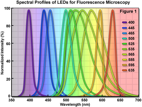
Compared to laser light, the wider bandwidth featured by LEDs is more useful for exciting a variety of fluorescent probes, and compared to the excessive heat and continuous spectrum emitted by arc lamps, LEDs are cooler, smaller, and provide a far more convenient mechanism to cycle the source on and off, as well as to rapidly select specific wavelengths. Commercial LED illumination units designed for fluorescence microscopy have been introduced by several manufacturers, and despite their weaker emission intensity when compared to the bright spectral lines of mercury and metal halide arc lamps, current trends in LED development point to the expectation of significant increases in brightness throughout all wavelength regions in the next few years. Furthermore, recent advances in LED technology targeted at producing die crystals having a geometry that decreases light loss through internal reflection should help generate devices that can be incorporated into virtually all applications in fluorescence microscopy. Illustrated in Figure 1 are the LED emission spectral profiles for several commercially available diodes. The spectra were recorded at the microscope objective focal plane using a broadband mirror positioned in a fluorescence optical block. Power levels for these LEDs are listed in Table 1 using both a mirror and common fluorescence filter sets.
In contrast to arc lamps, which exhibit a high degree of intrinsic radiance or brightness, LED technology has slowly evolved from rudimentary devices that were capable of providing only a thousandth of a lumen of red light in the late 1960s. During the past four decades, however, LEDs have advanced at a pace that rivals microprocessors. Similar to the prediction by Gordon E. Moore that the number of transistors on a computer chip would double every two years, Agilent Technologies scientist Roland Haitz predicted that the brightness of LEDs would increase by a factor of 20 every 10 years. In fact, what is now termed Haitz' Law has proven to be reliable because LEDs have historically doubled in brightness every two years and are expected to continue this dramatic growth in performance. As their brightness and the range of available colors has increased, LEDs have been put to use in a variety of new applications, including the role of an energy-efficient and durable replacement for incandescent lamps for home and industrial lighting. In addition, high-performance LEDs are now being used in a variety of other industrial, medical, and military applications. Among the many examples are navigation, robotics, machine vision, endoscopy, and diagnostic instrumentation. In the future, there should be an increasing demand for high brightness light sources based on LED devices in areas of the economy that have substantially more market power than optical microscopy. This demand will no doubt provide a driving force for the development of powerful LEDs emitting in all spectral regions, thus benefiting all illumination modalities in optical microscopy.
Many of the initial attempts to employ LEDs as light sources for microscopy failed in part because of the low radiant output of early devices. In general, the previously patented designs for microscope illumination were based on large numbers of LEDs grouped to generate a uniform pattern of illumination. This approach produced a relatively high radiant flux level, but failed to address the low radiance that results from such a large, distributed light source (in contrast to the point source characteristics of an arc-discharge lamp). Currently available high-performance LEDs are sufficiently bright to function individually as a highly effective source of monochromatic light having low spatial coherence for observations in fluorescence epi-illumination or with polychromatic light in transmitted microscopy. Although their averaged spectral irradiance is still lower than that of the spectral peaks from the powerful HBO (mercury) 100-watt arc-discharge lamp, it is approaching that of the XBO (xenon) 75-watt arc lamp continuum in many of the visible portions of the spectrum.
LEDs are considerably more efficient than arc-discharge lamps at converting electricity into visible light, often achieving outputs of up to 100 lumens per watt compared to the 22 lumens per watt for an HBO 100-watt source. These semiconductor devices are rugged and compact, and can often survive for 100,000 hours in use, or approximately 500 times longer than an HBO mercury lamp. Several of the green LEDs have conversion efficiencies as high as 75 percent, although devices in this wavelength range still suffer from reduced power output. In contrast, violet and blue LEDs having light outputs of 250 and 150 milliwatts, respectively, are now commercially available and similar powers in other wavelengths should be available in the near future. The output of LEDs can be modulated at high frequencies (up to 5 kilohertz) and their output brightness can be regulated by controlling the available current. These advantageous features eliminate the requirement for mechanical shutters as well as neutral density filters to control illumination of the specimen in microscopy applications. Although LEDs feature relatively narrow spectral emission profiles, in most cases they must still be used with interference thin-film excitation filters to remove the residual wavelengths on the extremes (at the spectral tails).
Optical Power of LEDs
|
||||||||||||||||||||||||||||||||||||||||||||||||||||||||||||||||||||||||||||||||||||||||||||||||||
Table 1
Presented in Table 1 are the optical output power values and FWHM spectral bandwidths for several near-ultraviolet and visible emitting LEDs that are currently used in fluorescence microscopy. The power for each LED is catalogued in milliwatts/cm2 and was measured at the output of a liquid light guide (LLG column in Table 1) as well as the focal plane of the microscope objective (40x fluorite dry, numerical aperture = 0.85) using a photodiode-based radiometer. Either a mirror with greater than 95% reflectivity from 350 to 800 nanometers or a standard fluorescence filter set was used to project light through the objective and into the radiometer sensor (values listed in columns labeled Mirror and Filter Set, respectively, in Table 1). The light throughput loss in a microscope illumination system can vary between 95 and 99 percent of the input power, depending upon the number of filters, mirrors, prisms, and lenses in the optical train. For a typical research-grade inverted microscope coupled to an external LED illumination source, less than 3 percent of the light exiting the liquid light guide is available for excitation of fluorophores positioned at the objective focal plane. A similar degree of light loss occurs with external metal halide light sources coupled to the microscope through a liquid light guide, as well as traditional xenon and mercury arc discharge lamps secured directly to the illuminator through a lamphouse.
In commercial LED lamphouses, individual diode modules can be readily interchanged to achieve excitation bandwidths suitable for the various fluorophores used in each experiment. The intensity of each LED module can also be independently adjusted in precise electrical steps (percentages of maximum output) so that illumination excitation periods can be balanced with detector sensitivity to avoid specimen phototoxicity. Another advantage of LEDs is their ability to instantly illuminate at full intensity once the electrical current is applied. Unlike arc-discharge and incandescent lamps, LEDs can be repeatedly modulated, or switched on and off, without suffering deleterious effects on their life span. Furthermore, without mechanical parts, the all-electronic diode illumination system is free of the problematic vibrations produced by shutter and neutral density filter motion.
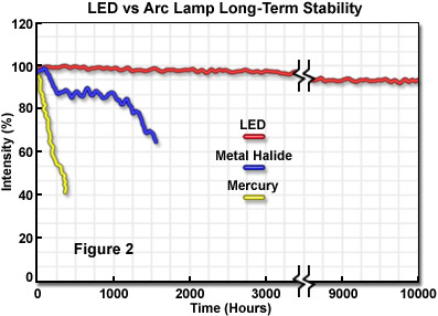
A unique aspect of LED illumination is the outstanding spatial and temporal stability (compared to traditional illumination sources), which enables highly accurate quantitative analysis techniques for extended periods. LEDs are governed by the fully reversible photoelectric effect during operation. As a result, LEDs feature the lowest operating temperatures of all light sources in optical microscopy and are among the most stable in temporal and spatial terms, as well as wavelength distribution. Furthermore, provided LEDs are operated at the proper voltage and current, they feature a significantly longer lifetime than any of the other currently available light sources (see Figure 2). Mercury and xenon arc lamps have a lifespan of 200 to 400 hours (respectively), whereas metal halide sources last 2,000 hours or more. Tungsten-halogen incandescent lamps have lifetimes ranging from 500 to 2,000 hours, depending on the operating voltage. In contrast, many LED sources exhibit lifetimes exceeding 10,000 hours without a significant loss of intensity, and some manufacturers guarantee a lifetime of 100,000 hours before the source intensity drops to 70 percent of the initial value.
All lamps that produce a significant level of heat, including LEDs, also exhibit a dependence of emission output on the source temperature. For incandescent and arc lamps, a period of up to one hour is required until the illumination source is sufficiently stable to enable reproducible measurements or to gather time-lapse video sequences without significant temporal variations in intensity. This long waiting period is not necessary for LEDs, which are capable of reacting extremely fast (within a few microseconds). However, the highest power versions can also generate a significant amount of heat (approaching 60 to 70 percent of their output) during warm-up and, due to their high speed, are affected by high-frequency instability in the power supply. When operating LEDs, a change in current can produce a shift of the emission peak that is similar in magnitude to that seen in the lines of arc lamps. This effect often occurs if the LED die is not perfectly homogeneous, and the size of the shift often depends on the type and quality of the semiconductor crystal used in fabricating the device. Wavelength stability can be ensured when using LEDs by calibrating the spectral output with operating current prior to initiating experiments.
Silicon diodes emit light in the near-infrared (IR) region, but diodes made from other semiconductors can emit in the visible and near-ultraviolet (UV) wavelengths. A typical LED source consists of a semiconductor crystal ranging from approximately 0.3 x 0.3 millimeters to 1 or 2 square millimeters in size. The most common crystals used in the fabrication of LEDs are based on mixtures of periodic table Group III and Group V elements, such as GaN (gallium nitride), SiC (silicon carbide), ZnSe (zinc selenide), and GaAlAsP (a mixture of gallium, aluminum, arsenic, and phosphorous). Each of these crystals emits in a different waveband (see Figure 1 and Table 2). Careful control of the relative semiconductor proportions, as well as the addition of dopants to alter the electronic properties of the crystalline lattice, enables manufacturers and researchers to produce diodes that emit red, orange, yellow, or green light. The spectral bandwidth of these emissions typically ranges between 12 and 40 nanometers with no significant out-of-band components in the infrared or ultraviolet wavelengths (spectral regions detrimental to live cell imaging). The application of silicon carbide and gallium nitride in LEDs has resulted in devices that emit in the blue region (useful for excitation of cyan, green, and yellow fluorescent protein variants), while combining several colors in different proportions can generate various color temperatures of white light for transmitted microscopy applications.
In a typical configuration for optical microscopy illumination, one or more dies are embedded into a larger LED structure for protection and more efficient light collection, as well as the ease of electrical connection and thermal handling. Among the primary advantages of LED technology is that small individual units can be combined to engineer a light source having the shape best suited to a particular application. Possible source geometries are limited only by heat dissipation and the permitted package density of the surface mount device (SMD) technology used to integrate a number of dies onto the printed circuit board. In this manner, very dense, bright, custom-designed light sources can be fabricated to match the input collection parameters of the target optical system. In microscopy, multiple LEDs can be packed into a compact and efficient internal or external light source that emits a high flux of quasi-monochromatic photons from a small area to completely fill the objective (or condenser) aperture.
Basic Properties of LEDs
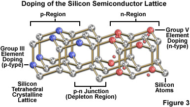
The fundamental characteristics of LEDs are distinct from those of other illumination sources commonly employed for optical microscopy. As such, LEDs comprise a unique category of non-coherent light sources that are capable of producing continuous and efficient illumination from a simple twin-element semiconductor diode (termed a chip or die) encased in a clear epoxy housing that, in many cases, also serves double duty as a projection lens. The overall concept surrounding LED operation is extremely simple. One of the two semiconductor regions in the chip is dominated by negative charges (the n region), while the other is dominated by positive charges (the p region). When sufficient voltage is applied to the electrical leads, a current is created as electrons transition across the junction between the two semiconductors from the n region into the p region where the negatively charged electrons combine with positive charges. The intermediate area or junction between the two semiconductors is known as the depletion region (see Figure 3). Each recombination of charges that occurs in the depletion region is associated with a reduction in energy level (equal to the charge times the band gap, V(g), of the semiconductor), which may release a quantum of electromagnetic radiation in the form of a photon having an energy (and wavelength) equal to the band gap energy. The wavelength bandwidth of emitted photons is a characteristic of the semiconductor material (see Table 2), therefore, different colors can readily be achieved by making changes to the semiconductor composition of the chip.
Light-Emitting Diode Color Variations
|
|||||||||||||||||||||||||||||||||||||||||||||||
Table 2
As semiconductor materials, LEDs have properties common to elements in the silicon category of the periodic table and display variable electrical conduction characteristics. Typical semiconductors exhibit electrical resistances values that are intermediate between those of conductors and insulators, and their behavior is modeled in terms of the electronic band theory for solids. In a crystalline solid, electrons occupy a large number of energy levels that are grouped together into nearly continuous energy bands, the width and spacing of which differ considerably with the specific properties of the material. At higher energy levels two distinct bands, termed the valence and conduction bands, are used to define the band gap for a particular material. Valence band electrons, which form fixed localized bonds between atoms in a solid, have lower energy than the highly mobile conduction band electrons. Conductors have overlapping valence and conduction bands that enable the transition of valence electrons into the conduction band to produce holes (vacancies with a net positive charge) in the valence band. Electrons from adjacent atoms can easily migrate through the lattice into holes, thus creating a movement of vacancies in the opposite direction. In contrast, insulators have fully occupied valence bands and much larger band gaps that require significant energy input in order to displace valence electrons into the conduction band.
The band gaps in semiconductors are small, but finite, and at room temperature, mere thermal agitation is sufficient to move some electrons into the conduction band. Most of the electronic devices incorporating semiconductors (such as diodes and transistors) are designed so that application of a voltage is required to produce the changes in electron distribution between the valence and conduction bands necessary to permit current flow. There are large differences in the band gap potential between different semiconductors, although the band arrangement is similar in all of these materials. Silicon, which is the simplest intrinsic semiconductor, does not have the appropriate band gap structure to be useful by itself in LED construction (but silicon is still used in many other devices, including integrated circuits). However, the conduction characteristics of silicon can be improved by doping (Figure 3), which introduces minute quantities of impurities to generate additional electrons or vacancies (holes) in the native crystalline structure.
The process of doping is best described using the element silicon, a Group IV member of the periodic table. Silicon has four valence electrons that participate in bonding with neighboring atoms in the pure crystal, leaving no deficit or excess. If a small amount of a Group III element (having three valence electrons) is mixed into solid silicon, an insufficient number of electrons are now available to satisfy all bonding requirements, creating holes in the crystal and producing a net positive charge to classify the doped silicon as a p-type semiconductor. Boron is one of the elements that is commonly utilized to dope pure silicon to achieve p-type characteristics. In contrast, adding a Group V element, such as phosphorus (having five valence electrons), to pure silicon generates an n-type semiconductor that has a net negative charge due to the extra valence electrons. The two most common semiconductor elements, silicon and germanium, are generally unsuitable for construction of LEDs due to the significant amount of heat produced at the junctions as well as their low emission levels of visible and infrared light.
Photon-emitting diode p-n junctions are typically based on a mixture of Group III and Group V elements, such as gallium, arsenic, phosphorous, indium, and aluminum. The relatively recent addition of silicon carbide and gallium nitride to this semiconductor palette has yielded blue-emitting diodes, which can be combined with other colors or secondary phosphors to produce LEDs that emit white light. The fundamental key to manipulating the properties of LEDs is the electronic nature of the p-n junction between two different semiconductor materials. When dissimilar doped semiconductors are fused, the flow of current into the junction and the wavelength characteristics of the emitted light is determined by the electronic character of each material. In general, current will readily flow in one direction across the junction, but not in the other, constituting the basic diode configuration. This type of behavior is best understood in terms of the transition of electrons and holes in the two materials and across the junction. Electrons from the n-type semiconductor move to the positively doped (p-type) semiconductor, which has vacant holes, allowing electrons to "jump" from hole to hole. The result of this migration is that holes appear to move in the opposite direction, or away from the positively charged semiconductor toward the negatively charged semiconductor. Electrons from the n-type region and holes from the p-type region recombine in the vicinity of the junction to form the depletion region (Figure 3), in which no charge carriers remain. Thus, a static charge is established in the depletion region that inhibits current flow unless an external voltage is applied.
In order to configure a diode, electrodes are placed on the opposite ends of a p-n semiconductor device to apply a voltage that is capable of overcoming the effects of the depletion region. Typically, the n-type region is connected to the negative terminal and the p-type region is connected to the positive terminal (known as forward biasing the junction) so that electrons will flow from the n-type material toward the p-type and holes will move in the opposite direction. The net effect is that the depletion zone disappears and electrical charge moves across the diode with electrons driven to the junction from the n-type material, whereas holes are driven to the junction from the p-type material. The combination of holes and electrons flowing into the junction enables a continuous current to be maintained across the diode. Although control of the interaction between electrons and holes at the p-n junction is a fundamental element in the design of all semiconductor diodes, the primary goal of LEDs is the efficient generation of light. The production of visible light due to injection of charge carriers across the p-n junction only takes place in semiconductor diodes having specific material compositions, which has led to the search for new combinations that feature the necessary band gap between the conduction band and orbitals of the valence band. Furthermore, research is ongoing to design LED architectures that minimize absorption of light by the diode materials and are more robust at concentrating light emission in a specific direction.
LED Construction
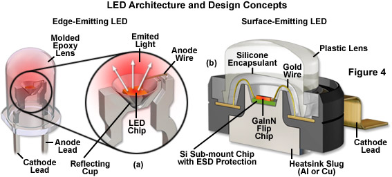
Among the critical aspects of LED fabrication are the nature of the elements used for the n-type and p-type semiconductors, as well as their physical geometry, design of the device housing, and configuration of the light escape route. The basic structure of a typical LED consists of the semiconductor material (the die or chip), a frame on which the die is mounted, and the encapsulation material surrounding the assembly (see Figure 4). In most cases, the LED semiconductor is supported in a reflector cup that is attached to an electrode (the cathode), while the top face of the chip is connected with a gold bonding wire to a second electrode (the anode). Several of the more complex junction structure designs require two bonding wires, one for each electrode. In addition to the obvious variation in the radiation wavelength of different LEDs, there are also variations in shape, size, and radiation pattern. Semiconductor LED chips range in size up to several square millimeters, and the housing/lens system varies between 2 and 10 millimeters in diameter. Most commonly, the BODY of the LED features a hemispherical geometry, but they may also be rectangular, square, triangular, or polygonal.
Presented in Figure 4 are the architectural details of two popular LED package designs. The conventional lead-frame hemispherical 5-millimeter LED featured in Figure 4(a) is commonly used as an indicator lamp for electronic appliances. Epoxy resins are used to cast the encapsulant system in these LEDs, which also feature cylindrical and rectangular lens geometries. The die is secured in a conical reflector cup that is soldered to the cathode lead and the anode is connected to the die with a bonding wire. Light emerging from the sides of the LED is reflected by the cup into the epoxy BODY. A flat cast into the base of the epoxy dome serves as an indicator of lead polarity. Typically, these indicator LEDs contain a die that measures 0.25 to 0.3 millimeters on the side, while the lens diameter ranges from 2 to 10 millimeters. The high-power GaInN flip chip diode cross section illustrated in Figure 4(b) is build on an aluminum or copper heat sink slug that can be soldered onto a printed circuit board for more efficient heat removal. Encapsulating the die is a protective silicone layer designed to overcome total internal reflection of emitted wavefronts and direct them through the larger plastic lens. A gold wire serves to connect the large cathode lead to the die, which is mounted on a silicon chip for protection against electrostatic discharge. The anode (not shown) is similar in configuration to the cathode, but projects away from the package in the opposite direction. LEDs of this design are currently the preferred choice for illumination in fluorescence microscopy.
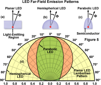
The emission color of an LED is determined by the combination of semiconductors used in the fabrication process, whereas the optical characteristics are generally controlled by variables in the packaging. The beam angle can range from narrow to wide (see Figure 5), and is determined by the shape of the reflector cup, the size and design criteria of the semiconductor, the distance from the chip surface to the top of the housing or lens system, and the geometry of the lens. LED emission profiles can generally be divided into two classes: edge emitters (Figure 4(a)) and surface emitters (Figure 4(b)). Most surface emitters exhibit a Lambertian emission pattern (see Figure 5(d)) where the intensity profile is proportional to the cosine of the emission angle, which is measured from the axis perpendicular to the die surface. In contrast, edge emitters typically emit light from a small region (approximately 50 micrometers in size) on the sides of the die in a complex pattern that is axis-dependent. The light escaping from an edge emitter is non-symmetrical, with a fast axis perpendicular to the lateral edge dimension, and a slow axis parallel to the die. In order to focus and collimate the light from all four sides of an edge-emitter LED, the die is usually housed inside a reflective cup (Figure 4(a)) at the expense of expanding the source size.
Illustrated in Figure 5(d) are far-field emission patterns for LEDs featuring planar (Figure 5(a)), hemispherical (Figure 5(b)), and parabolic (Figure 5(c)) lenses. The three emission patterns in Figure 5(d) are normalized and overlaid for comparison purposes. Note that at F=60°, the planar Lambertian diode emission pattern decreases to 50 percent of its maximum value, whereas the hemispherical LED features a more symmetrical distribution. Tinting that is applied to some epoxy lenses does not determine the emission color of an LED, but rather is used as a convenient indicator of the lamp color when inactive. LED designs targeted for applications that require high intensity (such as fluorescence microscopy) usually feature clear lenses without tint or diffusion additives. This configuration produces the greatest level of light output and is usually designed to feature a custom-shaped beam for the most efficient transfer of light into a collection or projection lens system. Alternatively, diffusion-type LED lenses contain embedded glass particles that spread the emitted light cone into a larger angle. This lens style is commonly employed in applications in which the LED is viewed directly, such as for indicator lamps on equipment panels.
The choice of materials and fabrication techniques for LED construction is guided by two primary targets: the maximization of light generation in the hybrid semiconductor materials and the efficient extraction of the light created by the device. In typical p-n junctions, electrons and holes from n-type and p-type materials (the majority carriers) are injected across the junction to establish the flow of current and to produce light (radiative recombination) in a specific wavelength band. This process is often hampered by non-radiative recombination of minority carriers (electrons in p-type materials and holes in n-type materials) with majority carriers. In addition, the presence of impurities, structural dislocations, and other crystalline defects in semiconductor materials can lead to non-radiative recombination events, which do not result in emission of a photon. Thus, one of the primary goals in LED design is to maximize the radiative recombination of charge carriers by careful selection of suitable semiconductor materials to provide the appropriate band structure in order to produce favorable quantum efficiency values. Another important goal, as discussed in greater detail below, is to ensure that the greatest possible amount of light generated by an LED is able to escape the device and be used for illumination.
The wavelength (and color) of light emitted by a semiconductor diode is determined by the difference in energy between the recombining electron-hole pairs of the valence and conduction bands, as previously described. The approximate energies of the carriers correspond to the upper energy level of the valence band and the lowest energy of the conduction band. As a result, the wavelength (l) of an emitted photon is approximated by the following expression:
l = hc/Ebg
where h represents Planck's constant, c is the velocity of light, and Ebg is the band gap energy. In order to modulate the wavelength of emitted radiation, the band bap of the semiconductor material utilized to fabricate the diode must be carefully selected. Gallium arsenide is a popular diode material and serves as an excellent example of how a semiconductor band structure can be altered to vary the LED emission wavelength. The band gap of gallium arsenide is approximately 1.4 electron-volts, which produces emission at approximately 900 nanometers, in the near-infrared region. In order to increase the frequency of emission to achieve wavelengths in the visible red region (650 nanometers), the band gap must be increased to approximately 1.9 volts. This can be accomplished by mixing gallium arsenide with a compatible material having a larger band gap (such as gallium phosphide; band gap of 2.3 electron volts). Thus, LEDs produced with the compound GaAsP (gallium arsenide phosphide) can be customized to produce band gaps having any value between 1.4 and 2.3 electron-volts through adjustment of the content ratio between arsenic and phosphorous. Other semiconductor combinations can be similarly applied to generate emission wavelengths spanning the near-ultraviolet, visible, and near-infrared spectral regions.
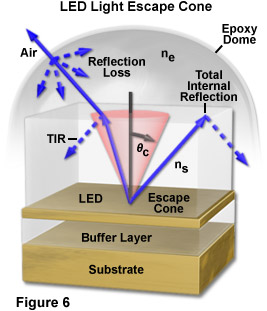
The efficient extraction of the light generated by an LED is another major issue in the fabrication of these semiconductor devices. As the bulk depletion region inside the LED die is an isotropic (Lambertian) emitter, it would generally be assumed that light leaving the front surface of the die would also be isotropic in all directions. However, because of total internal reflection phenomena, only a fraction of the light that is generated isotropically within the complete volume of a semiconductor chip is actually able to escape to the outside environment. In most cases, approximately 50 percent of the light generated internally is lost to reflections and other phenomena, and even less light is emitted at larger angles.
According to Snell's law, light can travel from a medium of higher refractive index into a medium of lower refractive index (in effect, from a semiconductor into the surrounding atmosphere) only if the exiting wavefronts intersect the interface between two media at an angle less than the critical angle for the two media. In a typical LED having a cubic geometry, only about 2 percent of the generated light is able to escape through the top surface (the actual value is dependent upon the specific semiconductor materials and p-n junction characteristics). The remainder is absorbed within the semiconductor, as described above. As an example, Figure 6 illustrates the escape of light from a layered semiconductor having refractive index ns into an epoxy lens of lower index (ne). The angle subtended by the escape cone is defined by the critical angle, qc, for the two materials. Light waves emerging from the LED at angles less than qc escape into the epoxy with minimal reflection loss, while those waves propagating at angles greater than qc undergo total internal reflection at the boundary and do not escape the device. Due to the curvature of the epoxy dome for the example in Figure 6, however, most light waves exiting the semiconductor material encounter the epoxy/air interface at nearly right angles and emerge from the housing with little reflection loss.
The amount of light emitted by an LED is dependent upon the number of surfaces through which the light can escape and how effectively this can occur at each surface. Nearly all LED structures are composed of a layered configuration in which epitaxial crystalline growth processes are employed to successively deposit a series of lattice-matched materials on top of one another to customize the properties of the chip. A wide variety of structural combinations can be used, with each system featuring a different layer architecture in order to optimize performance properties. In most cases a secondary growth step is required to deposit a single-crystal layer on the surface of a bulk-grown substrate material. Among the considerations necessary to ensure a high level of performance are the physical properties of the semiconductor materials, positioning of the p-n junction (where light emission occurs), and the stringent control of crystalline defects, all of which might raise or lower light generation efficiency.
Epitaxial crystal growth involves the liquid or chemical vapor deposition of one material onto another while attempting to reduce defects in the layered structure by preserving a close match in atomic lattice constants and thermal expansion coefficient. A number of techniques are used to produce epitaxial layers, including Liquid Phase Epitaxy (LPE), Vapor Phase Epitaxy (VPE), Metal-Organic Epitaxial Chemical Vapor Deposition (MOCVD), and Molecular Beam Epitaxy (MBE). Each methodology has particular advantages with regard to the optimum semiconductor materials and environmental production conditions. Among the many strategies behind the application of various layered semiconductor configurations are microstructuring of the p and n regions, junction parameters, reflective layer requirements to increase internal quantum efficiency, addition of graded-composition buffer layers (designed to overcome lattice mismatch between layers), and energy band gap targets to control the emission profile.
LED-based illumination sources targeted at microscopy utilize three different principles to reflect and gather the light generated inside the semiconductor die. The first and most common approach uses a transparent, molded plastic (polymer) to gather and focus the emitted light. Although suitable for low-level brightfield applications, this technique is not particularly useful in general microscopy due to the limited optical power available from a single diode. The second approach involves organizing a small array of LED dies directly onto a printed circuit board and using a customized collector optical system. The density of LED packaging is limited only by the need to bond each die with separate connection wires and to incorporate a mechanism to dissipate heat. The primary disadvantage of nested printed circuit LEDs is the loss of light that occurs from the edges of the devices. The third technique involves placing the LED die into a mirrored well that serves as a reflector, and then packing these units onto a printed circuit board. However, because the reflectors are larger than individual dies, this method results in a lower packing density.
Because every LED die constitutes an individual light source, when a large diode array is constructed using multiple devices, gathering the emitted light requires a different strategy than is employed with conventional lamps. The most efficient mechanism to collect light from nested LEDs involves the application of a microlens array that is positioned at the proper distance from the diode printed circuit board. A suitable lens array can be fabricated from molded plastic or glass and must be designed so that each LED has a separate collection lens. The microlens array then projects light from the individual sources into the macroscopic collector lens of the microscope optical train at a lower numerical aperture and longer focal length than would be required for a traditional lamp. As an added benefit, this type of optical system exhibits a lower degree of chromatic and spherical aberration. The primary design goal of a microlens-LED configuration (similar to that of any other illumination source) is to capture as much light as possible and efficiently deliver it into the acceptance angle of the microscope illumination optical system in order to completely and homogeneously fill the condenser (or objective) aperture diaphragm with axial, parallel light.
White Light LEDs
The most widely used current generation LEDs are fundamentally high-brightness monochromatic emitters, but an increasing number of applications (such as transmitted light microscopy) require broad spectrum or white light. There are two principal approaches for producing white light from devices that are basically monochromatic. One technique is based on combining three different diode colors in a single envelope, or different semiconductor materials in a common die (in such a proportion that the output appears white). The other method utilizes a violet or ultraviolet LED to provide energy that excites a secondary phosphor, which then emits white light (see Figure 7 (a)). White light LEDs are potentially very energy efficient compared to incandescent lamps. For example, whereas conventional light sources exhibit an average output of 15 to 100 lumens per watt, the efficiency of white LEDs is predicted to reach more than 300 lumens per watt as the result of continued development. Perhaps the most important criteria for white light LED selection is the average color temperature of the emission profile, which ranges from approximately 4500 K to 8000 K, depending upon the device properties. Choosing the best color match for optical microscopy should be based on the detector specifications and software capabilities, but values close to 5500 K should be optimal.
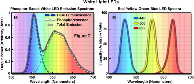
The combination of red, green, and blue diode dies into a single package, or in a lamp assembly housing a cluster of diodes, enables the generation of white light or any of the 256 colors by employing circuitry that drives the three diodes independently (Figure 7(b)). In applications that require the full spectrum of colors from a single point source, this type of RGB diode format is the preferred technique. However, most white light diodes are fabricated using a LED emitting at a short wavelength (365 to 450 nanometers; ultraviolet to blue) and a wavelength converter, which absorbs light from the diode and undergoes secondary emission at a longer wavelength. Such LEDs emit light of two or more wavelengths that when combined, appear as white. The quality and spectral characteristics of the combined emission vary with the materials used to construct the device. The most common wavelength-converter materials are termed phosphors, which are materials that exhibit luminescence when they absorb energy from another radiation source. Typically, phosphors are composed of an inorganic host substrate containing an optically active dopant. Yttrium aluminum garnet (YAG) is a common host material that can be doped with one of the rare-earth elements, such as Cerium.
LED Lamphouses
Among the advantages of using LEDs for illumination in fluorescence microscopy is that each variation of these semiconductor-based devices features a similar energy conversion efficiency with emission restricted to a narrow wavelength range, and LEDs operate at a much lower temperature than arc or incandescent lamps. As a result, far less electrical power is required to achieve the same optical output as a traditional light source. Furthermore, LEDs are significantly more compact than arc lamps and they can be bonded directly to a heat sink that is readily cooled with a small, computer-controlled fan. Such technology renders it possible to mount LED sources directly inside the microscope system, closer to the specimen, to potentially avoid the significant loss of light intensity (often exceeding 95 percent) that occurs with all light sources as they are projected through the optical train. Despite this high level of flexibility, it should be noted that LED-based sources absolutely require an efficient heat sink because operation above room temperature reduces their life expectancy and results in a loss of optical output efficiency.
The optical output of a typical LED (measured as the total radiant flux) is approximately proportional to the level of current applied to drive the device. LED power supply designs must account for the response time (on the order of microseconds), the non-linearity in the voltage-emission relationship, and the maximum recommended driving current. Another primary concern should address the intrinsic noise levels of LEDs, although these devices are far more stable (at least an order of magnitude) than tungsten halogen or arc lamps. Further considerations should include ability to rapidly switch or modulate LEDs for applications in microscopy. Even though the relationship between input current and light output can exhibit non-linearity, it can be precisely measured and the power supply calibrated accordingly. As an alternative, linear control can be achieved by pulse-width modulation, which controls the LED intensity by varying the amount of time a diode spends in the on state relative to the off state. Such a design enables modulating the intensity of light in a relatively repeatable manner by altering the drive current, thus eliminating the requirement for a shutter or neutral density filters.
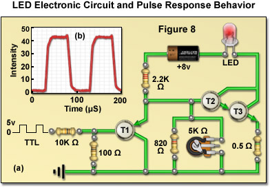
Presented in Figure 8(a) is a typical electronic circuit designed to drive a single surface-emitting blue LED that could be used in fluorescence illumination. The LED output intensity is adjusted using a potentiometer, and the emission can be toggled on and off by application of a switching signal derived from a low current, 5-volt TTL input (preferably originating from a host computer). In configuring a lamphouse for multiple LEDs, the safe maximum driving current for each diode must be taken into consideration. LEDs from the same batch (and distributor) can vary significantly (up to a volt) in their forward voltage drop, as well as other electrical properties, due to inherent manufacturing variations arising from a variety sources, including inhomogeneities in the raw materials. Thus, in order to maintain consistent performance between diode units it is necessary to predetermine the relationship between the holding voltage and current for each LED that will be used in a custom lamphouse. As an example of LED performance, the relationship between the response time of an LED to a square wave input is illustrated in Figure 8(b). Note how closely the LED output intensity follows the voltage step.
In situations where white light LEDs are required for broadband illumination, a single-channel current source can be used with the intensity and switching being controlled by altering the current flowing through one or more LEDs that have been matched for performance characteristics. In more advanced scenarios, complex LED configurations (combining several dies with different emission profiles) are used to obtain either narrow band emission for fluorescence or white light for brightfield illumination. These more sophisticated designs can be controlled through a multi-channel current source that is capable of altering intensity or emission wavelength on a microsecond (or even nanosecond) timescale. Termed pulse mode switching, this type of power supply is useful in technologies that require exceedingly short light bursts, such as lifetime imaging. The pulse mode scheme is useful to overcome shifts in peak emission wavelength due to LED heterogeneity by pre-adjusting each diode unit to the peak current necessary to produce the desired output wavelength. In this manner, the average source brightness can be regulated by varying the pulse width at a fixed peak current, thus ensuring controlled spectral output. As presented in Figure 8(b), the optical output follows the current pulse without significant delay and pulse-modulation frequencies ranging into the megahertz scale are possible.
Several commercial LED lamphouses have been introduced in the past several years for fluorescence and widefield transmitted (white light) microscopy, an example of which is illustrated in Figure 9. The lamphouse in Figure 9 is designed to couple directly with the microscope illuminator input port and houses up to four independently controllable modular LEDs for sequential or simultaneous excitation of multiple fluorophores. Individual LED modules can be readily interchanged to provide fluorescence excitation over the entire visible and ultraviolet spectrum. The modular design is intended to ensure that future LEDs, regardless of their configuration, can be made compatible for use in the lamphouse. Multicolor fluorescence images produced with this lamphouse (termed the Colibri and manufactured by ZEISS) feature very high contrast and a large dynamic range.
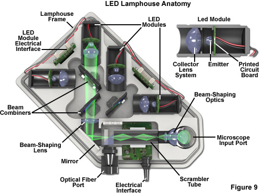
Among the advantages of the integrated LED lamphouse is the ability to set the illumination intensity for each diode to match the required camera integration time rather than using multiple camera settings. In addition, intensity control and switching of LEDs is purely electronic, thus eliminating mechanical shutters and filter wheels for greater speed and vibrational stability. The low head output of LEDs, which covert electricity into light with high efficiency as discussed above, eliminates the need for fans or auxiliary cooling devices. Furthermore, as LEDs are not under high pressure, their failure mode is harmless (no explosions) compared to arc lamps.
Contributing Author
Michael W. Davidson - National High Magnetic Field Laboratory, 1800 East Paul Dirac Dr., The Florida State University, Tallahassee, Florida, 32310.