


Among the most promising of emerging technologies for illumination in optical microscopy is the light-emitting diode (LED). These versatile semiconductor devices possess all of the desirable features that incandescent (tungsten-halogen) and arc lamps lack, and are now efficient enough to be powered by low-voltage batteries or relatively inexpensive switchable power supplies. The diverse spectral output afforded by LEDs makes it possible to select an individual diode light source to supply the optimum excitation wavelength band for fluorophores spanning the ultraviolet, visible, and near-infrared regions. This interactive tutorial explores how two dissimilar doped semiconductors can produce light when a voltage is applied to the junction region between the materials.
The tutorial initializes with an animated image of a light-emitting diode semiconductor in the process of generating green light (535 nanometers). A positive voltage has been applied to the p-doped layer, whereas a negative voltage is applied to the n-doped layer. Beneath the semiconductor is a mirror substrate to reflect emitted photons. To operate the tutorial, use the Wavelength Selector slider to alter the emission wavelength and the Voltage Output slider to adjust the junction voltage and number of photons being emitted.
Photon-emitting diode p-n junctions are typically based on a mixture of Group III and Group V elements, such as gallium, arsenic, phosphorous, indium, and aluminum. The relatively recent addition of silicon carbide and gallium nitride to this semiconductor palette has yielded blue-emitting diodes, which can be combined with other colors or secondary phosphors to produce LEDs that emit white light. The fundamental key to manipulating the properties of LEDs is the electronic nature of the p-n junction between two different semiconductor materials. When dissimilar doped semiconductors are fused, the flow of current into the junction and the wavelength characteristics of the emitted light are determined by the electronic character of each material. In general, current will readily flow in one direction across the junction, but not in the other, constituting the basic diode configuration. This type of behavior is best understood in terms of the transition of electrons and holes in the two materials and across the junction. Electrons from the n-type semiconductor move to the positively doped (p-type) semiconductor, which has vacant holes, allowing electrons to "jump" from hole to hole. The result of this migration is that holes appear to move in the opposite direction, or away from the positively charged semiconductor toward the negatively charged semiconductor. Electrons from the n-type region and holes from the p-type region recombine in the vicinity of the junction to form the depletion region, in which no charge carriers remain. Thus, a static charge is established in the depletion region that inhibits current flow unless an external voltage is applied.
In order to configure a diode, electrodes are placed on the opposite ends of a p-n semiconductor device to apply a voltage that is capable of overcoming the effects of the depletion region. Typically, the n-type region is connected to the negative terminal and the p-type region is connected to the positive terminal (known as forward biasing the junction) so that electrons will flow from the n-type material toward the p-type and holes will move in the opposite direction. The net effect is that the depletion zone disappears and electrical charge moves across the diode with electrons driven to the junction from the n-type material, whereas holes are driven to the junction from the p-type material. The combination of holes and electrons flowing into the junction enables a continuous current to be maintained across the diode. Although control of the interaction between electrons and holes at the p-n junction is a fundamental element in the design of all semiconductor diodes, the primary goal of LEDs is the efficient generation of light. The production of visible light due to injection of charge carriers across the p-n junction only takes place in semiconductor diodes having specific material compositions, which has led to the search for new combinations that feature the necessary band gap between the conduction band and orbitals of the valence band. Furthermore, research is ongoing to design LED architectures that minimize absorption of light by the diode materials and are more robust at concentrating light emission in a specific direction.
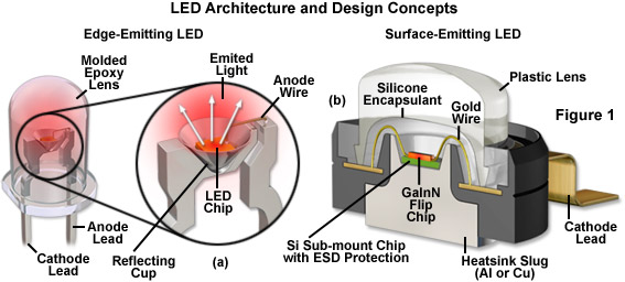
Presented in Figure 1 are the architectural details of two popular LED package designs. The conventional lead-frame hemispherical 5-millimeter LED featured in Figure 1(a) is commonly used as an indicator lamp for electronic appliances. Epoxy resins are used to cast the encapsulant system in these LEDs, which also feature cylindrical and rectangular lens geometries. The die is secured in a conical reflector cup that is soldered to the cathode lead and the anode is connected to the die with a bonding wire. Light emerging from the sides of the LED is reflected by the cup into the epoxy BODY. A flat cast into the base of the epoxy dome serves as an indicator of lead polarity. Typically, these indicator LEDs contain a die that measures 0.25 to 0.3 millimeters on the side, while the lens diameter ranges from 2 to 10 millimeters. The high-power GaInN flip chip diode cross section illustrated in Figure 1(b) is build on an aluminum or copper heat sink slug that can be soldered onto a printed circuit board for more efficient heat removal. Encapsulating the die is a protective silicone layer designed to overcome total internal reflection of emitted wavefronts and direct them through the larger plastic lens. A gold wire serves to connect the large cathode lead to the die, which is mounted on a silicon chip for protection against electrostatic discharge. The anode (not shown) is similar in configuration to the cathode, but projects away from the package in the opposite direction. LEDs of this design are currently the preferred choice for illumination in fluorescence microscopy.
Contributing Authors
Tony B. Gines and Michael W. Davidson - National High Magnetic Field Laboratory, 1800 East Paul Dirac Dr., The Florida State University, Tallahassee, Florida, 32310.